ASML (ASML) is a publicly traded Lithography & Equipment company founded in 1984 and based in Veldhoven, Netherlands.
| Date | Stage | Amount | Valuation | Lead investors |
|---|---|---|---|---|
| Feb 1, 1995 | IPO | $170M | — | — |

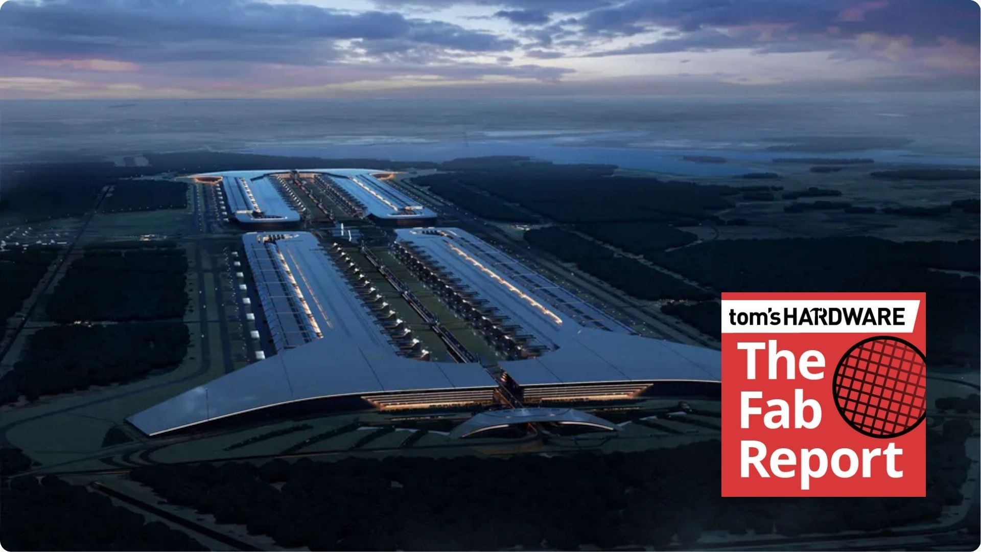
Musk says ASML and other equipment suppliers expedited shipments to the Terafab fab, targeting volume chip output by Q3-Q4 2028.

ASML reports record Q3 2026 revenue of $13.06B, up 55% year over year, with demand expected to exceed 2027 and 2028 capacity.

ASML customers are requesting more EUV lithography tools than planned for 2027 and 2028, with ASML investigating added capacity.

Terafab reportedly receives its first ASML EUV tool in mid-2027, but the scanner will sit idle until its development fab shell is finished in late 2027.

ASML plans to expand capacity to meet rising demand for its EUV lithography systems.
Extreme ultraviolet lithography scanners using 13.5nm light to pattern the smallest features on leading-edge logic and memory chips at 7nm and below. Each NXE-series machine costs roughly $150–200M and is essential for TSMC, Samsung, and Intel's most advanced nodes. ASML is the world's sole supplier of production EUV, making these systems the critical chokepoint in advanced chip manufacturing.
Next-generation EUV systems with a 0.55 numerical-aperture optical design that prints finer features in a single exposure, extending Moore's Law toward the 2nm era and beyond. Priced around $350M+ each, the EXE platform began shipping to leading customers including Intel and TSMC. High-NA EUV is ASML's most advanced product and a multi-year competitive moat in lithography.
Deep ultraviolet immersion and dry scanners (NXT/XT lines using 193nm light) that pattern mainstream and mature semiconductor nodes for logic, memory, automotive, and analog chips. DUV represents the high-volume backbone of ASML's installed base and remains central to export-control disputes over sales to China. The systems deliver high throughput and overlay accuracy for cost-sensitive production.
Optical and e-beam metrology and inspection tools (largely from the HMI acquisition) plus computational-lithography software that optimize patterning and detect defects across the fab. Combined with ASML's holistic-lithography portfolio, these products improve yield and process control for EUV and DUV production, broadening ASML beyond scanners into a fuller fab-equipment and software supplier.