Semiconductors
Semiconductors
The next edition is being prepared. Check back shortly.
Subscribe for the full sector dashboard
Including The tracked-40 roster, Funding timeline, Valuations, Catalyst calendar, Latest news + videos, Talent moves, and Patent activity.
Already subscribed? Sign in →
Companies
- All subsectors
- AI Accelerators
- EDA & IP
- Edge AI
- Foundries
- Lithography & Equipment
- Memory
- Networking & Custom Silicon
- Photonics & Interconnects
- Power & Analog
- All statuses
- Private
- Public
- Relevancy
- Total raised
- Latest round
- Name
Cerebras builds wafer-scale AI chips with millions of cores optimized for large-scale model training and inference.
Etched builds application-specific chips hardwired to run transformer architectures with extreme performance and efficiency.
Groq builds Language Processing Units (LPUs) for ultra-low-latency LLM inference — the tech behind Nvidia's reported ~$20B Dec 2025 IP deal.
Rebellions is a Korean AI-chip unicorn behind the ATOM and REBEL inference accelerators, formed by its 2024 merger with SK Telecom's Sapeon.
SambaNova builds dataflow AI accelerators and full-stack software for enterprise AI training and inference at scale.
d-Matrix builds in-memory compute chips optimized for efficient transformer inference at scale in data centers.
MatX, founded by ex-Google TPU engineers, designs chips optimized specifically for large language models, with first silicon due in 2027.
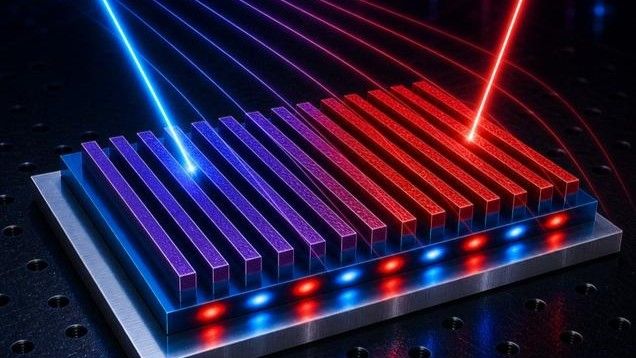
Ayar Labs develops chiplet-based optical I/O solutions that replace electrical interconnects in AI and HPC systems.
SiFive licenses RISC-V processor IP and builds custom silicon solutions for AI, automotive, and data-center customers.
Positron AI builds energy-efficient LLM inference appliances (Atlas) as a US-made, memory-bandwidth-optimized alternative to GPUs.
Axelera AI is a European edge-AI startup whose Metis chips use in-memory computing to run computer-vision inference at low power and cost.
FuriosaAI is a Korean startup building energy-efficient AI inference chips (RNGD); it rebuffed an ~$800M Meta buyout to stay independent.
Mythic develops analog compute-in-memory chips for edge AI inference, targeting industrial, defense, and automotive applications.
Lightmatter builds photonic processors and optical interconnects to accelerate AI compute and reduce data-center power consumption.
Astera Labs builds high-speed connectivity silicon — retimers, CXL controllers, and fabric switches — for AI and cloud data centers.
GlobalFoundries operates fabs focused on specialty and mature-node semiconductors for automotive, IoT, and RF applications.
SiMa.ai builds a software-centric edge-AI 'MLSoC' that runs computer-vision and ML workloads at low power for the embedded edge.
Hailo builds edge AI processors optimized for computer vision and neural network inference in automotive and industrial devices.
Arm licenses CPU architectures and IP used in nearly every mobile device and increasingly in data-center and AI chips.
Tenstorrent designs open-source RISC-V AI processors and licenses chiplet IP for scalable AI compute.
EnCharge AI develops in-memory compute chips for ultra-efficient AI inference at the edge and in data centers.
Navitas manufactures gallium nitride (GaN) power semiconductors that increase efficiency in data-center power supplies and AI systems.
Broadcom designs custom AI accelerators for hyperscalers (Google TPU) and supplies networking silicon critical to AI cluster interconnects.
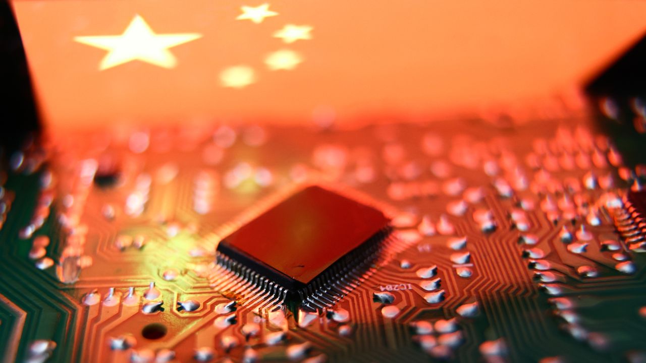
TSMC is the world's largest contract chipmaker, manufacturing over 90% of the world's most advanced chips including Nvidia and Apple silicon.
ASML holds a global monopoly on extreme ultraviolet (EUV) lithography systems required to manufacture chips at 7nm and below.
Marvell designs custom AI silicon for hyperscalers and supplies data-center networking, storage, and interconnect chips.
Qualcomm designs mobile SoCs, edge AI chips, and automotive silicon, bringing AI inference to devices outside the data center.
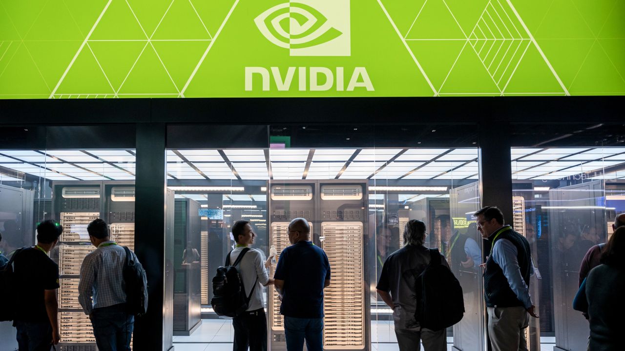
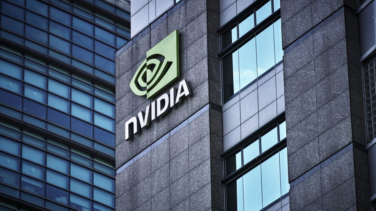
Nvidia designs GPUs and AI accelerators that power the vast majority of frontier model training and inference workloads.
AMD designs CPUs and AI accelerators including the MI300 series, competing directly with Nvidia in data-center AI workloads.
Intel designs x86 CPUs and operates Intel Foundry Services, pursuing both internal products and third-party manufacturing at scale.
Applied Materials is the largest semiconductor equipment maker, supplying deposition, etching, and metrology tools to every major fab.
Ambarella (NASDAQ: AMBA) designs low-power edge-AI vision SoCs — CV3-AD and N1 — for automotive ADAS, security cameras, and robotics.
Cadence provides EDA software and system design tools used to design advanced chips, boards, and systems across the semiconductor industry.
KLA provides process control and yield management systems that inspect and measure defects during semiconductor manufacturing.
Lam Research supplies etch and deposition equipment essential for manufacturing advanced logic and memory chips.
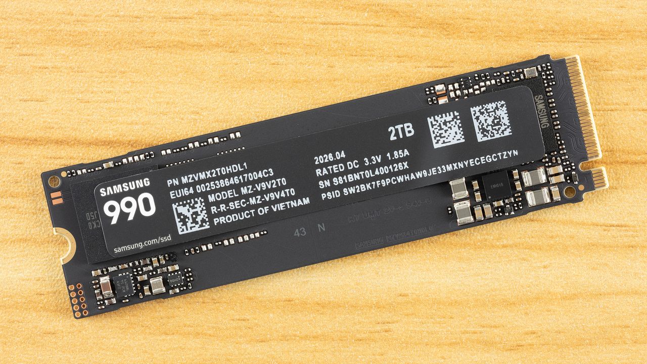
Micron produces DRAM, NAND, and HBM for AI and data-center applications, competing with Samsung and SK Hynix.
Samsung operates the world's second-largest semiconductor foundry and manufactures memory, competing with TSMC and SK Hynix.
SK Hynix manufactures high-bandwidth memory (HBM) that sits on every leading AI accelerator, plus DRAM and NAND for data centers.
Synopsys provides electronic design automation (EDA) software and IP that nearly every chip company uses to design semiconductors.
Tokyo Electron supplies deposition, etch, and cleaning equipment to semiconductor fabs, ranking second globally in wafer fab equipment.
KPIs
- 01Micron461
- 02Qualcomm451
- 03Applied Materials317
- 01Cerebras$8.3B
- 02Arm$4.9B
- 03GlobalFoundries$2.6B
Latest News
2d·Launch·positiveIntel Xeon 6+ Computex roundtable interview transcript — Kira Boyko and Tim Wilson on 18A wafer allocation, Clearwater Forest, and dropping hyper-threading
Intel launches Xeon 6+ processors at Computex with 18A node support and hyper-threading removal.
Tom's Hardware ↗
2d·Other·positiveSK hynix to double memory wafer capacity within five years, chairman says — AI-driven shortage will persist until at least 2030
SK Hynix plans to double memory wafer capacity within five years to address AI-driven demand extending through 2030.
Tom's Hardware ↗
2d·Launch·positiveJensen Huang says Nvidia wants to 'reinvent the single most important tool of humanity' with RTX Spark — Nvidia CEO touts support of 'literally every computer maker in the world' for its agentic AI PC platform
Nvidia CEO Jensen Huang announces RTX Spark, an agentic AI PC platform claiming support from major computer makers.
Tom's Hardware ↗
2d·Launch·neutralAMD ‘had to re-engineer’ the Ryzen 7 5800X3D for a re-release — 10th Anniversary Edition chip had ‘a whole body of engineering work’ put into it
AMD re-engineers the Ryzen 7 5800X3D for a 10th Anniversary Edition release after TSMC's original bonding process became unavailable.
Tom's Hardware ↗
2d·Launch·neutralIntel Arc G3 interview transcript — Intel's Senior Product Director talks new handheld chips, Arrow Lake Refresh, and RTX Spark
Intel's Senior Product Director discusses the Arc G3 chip line for handheld gaming, Arrow Lake Refresh, and RTX Spark at Computex 2026.
Tom's Hardware ↗
2d·Other·neutralIntel says 'something has to give' with memory prices — company says it 'will continue to make sure that there are products which can take care of older memory technologies'
Intel acknowledges persistent memory pricing pressures and commits to supporting legacy DDR4 platforms.
Tom's Hardware ↗
2d·Regulation·negativeChinese military has been acquiring Nvidia chips, even post-Washington export controls, research claims — multiple institutions linked to the PLA asked for Nvidia AI chips, according to publicly available documents
Research alleges Chinese military institutions have acquired Nvidia AI chips in violation of U.S. export controls, citing publicly available procurement documents.
Tom's Hardware ↗
2d·Demo·neutralThe Evolution Of UCIe
Cadence outlines the evolution of UCIe (Universal Chiplet Interconnect Express) as a comprehensive standard for chiplet packaging and multi-foundry integration.
Semiconductor Engineering ↗
2d·Research·neutralChip Industry Technical Paper Roundup: Jun. 2
Micron, Samsung, and AMD contribute to semiconductor research papers on inference scaling, memory reliability, and GPU power management.
Semiconductor Engineering ↗
2d·Demo·neutralIntel Computex 2026 Keynote Live Coverage
Intel CEO Lip-Bu Tan presents the company's AI hardware strategy at Computex 2026 keynote.
ServeTheHome ↗
3d·Demo·neutralMarvell Computex 2026 Keynote Live Coverage
Marvell CEO Matt Murphy addresses Computex 2026 keynote on connectivity solutions for AI data centers.
ServeTheHome ↗
3d·Launch·neutralAMD Radeon RX 9070 GRE review: thoroughly midrange
AMD launches the Radeon RX 9070 GRE at $549, a midrange GPU with strong 1080p and 1440p gaming performance.
Tom's Hardware ↗
Videos
Talent Moves
- May 14, 2026Andrew FeldmanCo-founder & CEOFromCo-founder & CEO (private)at Cerebras SystemsCNBCToCo-founder & CEO (public)at Cerebras Systems (CBRS)
Lam Research Newsroom ↗Mar 6, 2026Sesha VaradarajanSVP, Global Products Group- Feb 24, 2026Rodrigo LiangCo-founder & CEOFromCo-founder & CEOat SambaNova SystemsCNBC ↗ToCo-founder & CEO (post-Intel partnership)at SambaNova Systems
TechCrunch ↗Dec 24, 2025Jonathan RossFounder & CEO AdTechToday ↗Dec 24, 2025Sunny MadraPresident- Aug 1, 2025David ReederCFOFromChief Financial Officerat EntegrisSEC 8-K ↗ToPresident & CEOat Entegris
- May 1, 2025Rahul PatelIndustry ExecutiveFromSenior executiveat Qualcomm / BroadcomSEC 8-K ↗ToPresident & CEOat Synaptics
- Mar 18, 2025Lip-Bu TanFormer CEO of Cadence Design SystemsIntel Newsroom ↗FromExecutive Chairman (prior CEO 2009–2021)at Cadence Design Systems
- Jan 29, 2025Chen FengExecutive at Rockchip ElectronicsFromSenior Executiveat Rockchip ElectronicsBloomberg ↗ToChief Executive Officerat Arm China
- Dec 1, 2024Pat GelsingerCEOCNBC ↗ToRetiredat Independent
Tenstorrent Newsroom ↗Jan 1, 2023Jim KellerCTO
Catalysts
Conferences
Major industry dates · soonest first
Earnings Calls
Public roster companies · forecast from SEC filings
- Jun 17, 2026· rumoredMicron — Q2 2026 earnings
- Jul 23, 2026· rumoredIntel — Q2 2026 earnings
- Jul 27, 2026· rumoredCadence — Q2 2026 earnings
- Jul 29, 2026· rumoredQualcomm — Q2 2026 earnings
- Jul 29, 2026· rumoredLam Research — Q2 2026 earnings
- Jul 30, 2026· rumoredKLA — Q2 2026 earnings
- Aug 4, 2026· rumoredNavitas — Q2 2026 earnings
- Aug 4, 2026· rumoredAMD — Q2 2026 earnings
- Aug 13, 2026· rumoredApplied Materials — Q2 2026 earnings
- Aug 19, 2026· rumoredNvidia — Q3 2026 earnings
- Aug 27, 2026· rumoredSynopsys — Q3 2026 earnings
- Aug 28, 2026· rumoredMarvell — Q3 2026 earnings
Predictions
Public claims with deadlines
Nothing on the calendar yet.
Policy & Courts
Hearings · rulings · statutory deadlines
Nothing on the calendar yet.
Venture Stages
- —
- —
Valuations
Funding
Bottlenecks
Stochastic defects in High-NA EUV patterning
High-NA EUV (NA=0.55) shrinks the depth-of-focus so aggressively that resist thickness must drop below 30 nm, which dramatically increases stochastic effects — photon shot noise and secondary-electron blur can produce random missing or bridging features at the 2 nm node and below. Electron blur alone is estimated at ≥2 nm, which can cancel out the resolution benefit of High-NA optics. Achieving the defect densities needed for HVM on sub-2 nm nodes without sacrificing throughput is unsolved.
Stochastic defects in High-NA EUV patterning
ASML, Inpria (acquired by JSR), and academic partners at imec are developing metal-oxide resists that absorb EUV photons more efficiently per nm of thickness, reducing stochastic noise. Results are promising in the lab but HVM-grade yields are not yet demonstrated.
Synopsys and Cadence have both launched High-NA-aware optical proximity correction engines; the asymmetric pupil of High-NA tools creates new pattern-distortion modes that classical OPC does not model. Intel (the first chipmaker to receive production High-NA tools) is co-developing models with ASML.
TSMC and Samsung are each exploring complementary patterning schemes that use multiple lower-dose exposures to average out stochastic variation, at the cost of throughput. IBM Research has published results on stochastic-risk prediction models to guide exposure strategy.
Thermal management in vertically-stacked CFET transistors
Complementary FETs (CFETs) stack n-type and p-type transistors directly on top of each other to extend area scaling beyond the 2 nm node. The resulting heat density in a buried stack — with no direct path to a heat spreader — creates a thermal management problem that classical cooling cannot solve at production yields. Self-heating degrades carrier mobility and accelerates electromigration in buried interconnects.
Thermal management in vertically-stacked CFET transistors
Intel's 18A node introduced backside power delivery (PowerVia), partly to free front-side metal layers for thermal vias. Intel, Samsung, and imec are all researching whether backside thermal extraction structures can sufficiently cool CFETs without unacceptable process complexity.
Samsung and IBM are collaborating on monolithic CFETs, where both device tiers are built in one process flow, minimizing parasitic capacitance but maximizing thermal challenge. TSMC and imec favor sequential CFET (two separate bond-and-transfer steps) which offers better thermal handling but alignment tolerance issues.
Applied Materials and Lam Research are developing new dielectric fill processes with higher thermal conductivity to conduct heat laterally out of the CFET stack before it reaches the buried oxide.
Breaking the memory bandwidth wall for AI accelerators
TOPS/FLOPS performance in AI chips has outpaced DRAM bandwidth by roughly 2000× over the past two decades, leaving compute units idle while waiting for data. LLM inference is almost entirely memory-bandwidth-bound, meaning raw silicon throughput no longer translates to real-world speed. HBM stacking helps but is cost-constrained, and physical limits cap per-stack bandwidth below what next-generation model sizes demand.
Breaking the memory bandwidth wall for AI accelerators
SK Hynix, Samsung, and Micron are all ramping HBM4 for production in late 2026, targeting bandwidths above 1.65 TB/s per stack with 3nm logic base dies. TSMC and partner GUC have detailed C-HBM4E with 12.8 GT/s by 2027, but each generation requires foundry-class logic in the memory base die — tightly coupling logic scaling to memory bandwidth progress.
Encharge AI and d-Matrix are building inference accelerators that embed computation inside or immediately adjacent to the memory array to eliminate data movement. IBM Research has demonstrated analog AI inference chips using phase-change memory; Mythic's approach embeds weights in analog flash. None have yet matched the programmability of GPU/ASIC combos at production scale.
Ayar Labs and Lightmatter (both on the FOBI roster) are building optical I/O chiplets that embed silicon-photonics transceivers directly into the accelerator package, targeting terabits-per-second of off-chip bandwidth at dramatically lower energy per bit than copper SerDes.
Yield and reliability at extreme chiplet package scales
Chiplet architectures using CoWoS, EMIB, or hybrid bonding now routinely stitch together 10+ dies on a single interposer. As packages grow beyond 10 reticle-fields (TSMC's roadmap shows 14+ reticle CoWoS by 2029), the probability of a defect on any one die that kills the entire package grows toward unacceptable levels. Known-good-die (KGD) testing and repair are unsolved at the density and interconnect pitch of hybrid bonding.
Yield and reliability at extreme chiplet package scales
Nvidia's GB200 NVL72 rack-scale architecture partially sidesteps single-die yield by treating the rack as the unit of sale, but this does not solve per-package yield. KLA and Applied Materials are developing post-bond inspection tools capable of detecting sub-micron hybrid-bond defects non-destructively.
UCIe 2.0 and Open Compute Project chiplet consortia aim to create a market in known-good interchangeable dies so that failed chiplets can be swapped before final assembly. Broadcom, Intel, AMD, and Qualcomm are the largest contributors; Alphawave Semi builds UCIe PHY IP.
On-chip and rack-level power delivery for megawatt AI clusters
Next-generation AI accelerator modules are approaching 15 kW per module, and full NVL-class racks can exceed 100 kW. Delivering clean, stable voltage to billions of transistors switching at GHz rates across this power envelope — while managing electromagnetic interference, voltage droop, and thermal load — represents a fundamentally new power engineering problem that neither traditional VRM design nor on-package decoupling capacitors can fully solve.
On-chip and rack-level power delivery for megawatt AI clusters
Intel's PowerVia / 18A and TSMC's equivalent backside power research route power through the silicon substrate rather than front-side metal layers, cutting IR drop and freeing routing resources. Volume products using this architecture are expected in 2026–2027.
Navitas Semiconductor and a cluster of GaN power-IC startups are developing gallium-nitride VRMs that can switch at 10–100× the frequency of silicon MOSFETs, shrinking output capacitance requirements and enabling per-chiplet power domains.
Applied Materials, Tokyo Electron, and Intel Labs have published roadmaps for microfluidic cooling channels embedded in advanced package substrates, removing heat at the source rather than relying on air or external liquid cooling loops.
EDA scalability for trillion-transistor designs
Modern AI SoCs now contain tens of billions of transistors; roadmaps point to trillion-transistor packages within this decade. Classical EDA algorithms (place-and-route, formal verification, static timing analysis) scale poorly — verification of a trillion-transistor design is computationally intractable with current methods. AI-assisted design automation is necessary but not yet proven to close gaps in signoff quality.
EDA scalability for trillion-transistor designs
Cadence (Cerebrus AI) and Synopsys (DSO.ai) have both shipped AI-augmented PnR tools that use reinforcement learning to optimize floor plans. Siemens EDA is integrating similar capabilities; results show 10–20% QoR improvements on benchmark designs but generalization to novel architectures is unproven.
Cadence and Synopsys are both investing in learned abstraction layers that reduce the state-space for formal verification. Academic collaboration between MIT, Stanford, and major IDMs is exploring whether LLMs can generate useful property specifications to guide coverage.
Arm's Neoverse compute subsystem and SiFive's IP portfolio are designed to be assembled chiplet-style with pre-verified physical interfaces, reducing the per-design verification burden. Rivos (RISC-V server CPU startup) is pursuing a similar disaggregated verification strategy.
Investment Theses
AI creates a multi-decade GPU/accelerator supercycle
Frontier model training and inference demand is scaling faster than any prior compute wave — faster than mobile, faster than cloud. The TAM for AI accelerators is not the existing $50B data-center chip market; it is a replacement of every compute workload over 20 years as model inference becomes the dominant form of computing. Nvidia's 80%+ share in AI training, its CUDA ecosystem moat, and its roadmap cadence (Blackwell → Rubin → Feynman at one-year intervals) suggest the incumbent is also best positioned to extend the supercycle.
AI creates a multi-decade GPU/accelerator supercycle
AI compute demand could saturate if model architectures shift toward efficiency (MoE, distillation, test-time compute rather than training scale). ASIC alternatives from hyperscalers (Google TPU, AWS Trainium, Microsoft Maia) are increasingly capable and vertically integrated, squeezing merchant silicon share precisely where margins are highest.
Every hyperscaler builds its own chip — the death of merchant silicon at the top
Google, Amazon, Microsoft, and Meta have collectively spent tens of billions developing custom AI accelerators and Arm-based CPUs. The thesis is that at sufficient scale, the TCO advantage of a chip tailored to your workload and software stack dwarfs the R&D cost — and that the merchant silicon market will be bifurcated into commodity tiers for the long tail and custom silicon for the top 10 buyers who represent 70%+ of hyperscale spend. Arm architecture (IP from Arm Holdings) is the connective tissue, enabling custom silicon without a full ISA development cost.
Every hyperscaler builds its own chip — the death of merchant silicon at the top
Custom silicon has enormous non-recurring engineering costs and requires software retooling across entire ML frameworks. Most enterprise and mid-market cloud buyers cannot justify the investment, keeping merchant GPU/CPU markets healthy. Arm ISA fragmentation also creates portability overhead that generic platforms avoid.
Geopolitics fractures the foundry market into sovereign supply chains
TSMC's concentration in Taiwan — which produces 90%+ of the world's leading-edge logic — is an existential supply-chain risk that Western governments have concluded they cannot accept. CHIPS Act subsidies, EU Chips Act, Japan's Rapidus program, and India's semiconductor push all bet that subsidized geographic diversification of leading-edge fab capacity is worth a 30-50% cost premium. The TAM logic: if you can capture government-mandated or security-driven wafer demand, you don't compete on cost — you compete on sovereignty.
Geopolitics fractures the foundry market into sovereign supply chains
Geopolitically-motivated fabs cost 2-3× as much to build and operate as Taiwan equivalents. Government subsidies distort economics but don't close the gap fully. If China-Taiwan tensions defuse, the sovereign premium evaporates and high-cost fabs become stranded assets. The past track record of industrial-policy semiconductor programs (Sematech, EU fab initiatives) is poor.
Chiplets + UCIe create a semiconductor platform layer analogous to iOS/Android
The end of monolithic die scaling forces disaggregation: chips become assemblies of specialized chiplets (compute, memory, I/O, analog) connected by standardized interfaces. UCIe 2.0 and 3D-native packaging (CoWoS, EMIB, hybrid bonding) are the plumbing. The bet is that whoever owns the dominant chiplet interconnect standard and advanced packaging supply owns a Microsoft-of-silicon platform: capturing value from every chiplet that ships, not just the chiplets they design. Advanced packaging capacity is already the binding constraint on AI accelerator supply.
Chiplets + UCIe create a semiconductor platform layer analogous to iOS/Android
Chiplet standards have historically fragmented (PCIe, CXL, UCIe are all competing or complementary). Hyperscalers building proprietary chiplet assemblies may choose proprietary interconnects that don't comply with UCIe, keeping the market fragmented and preventing a dominant platform from emerging. 3D packaging yield problems also limit how aggressively the market can scale.
AI inference moves to the edge — a second silicon gold rush at device scale
Latency, privacy, bandwidth cost, and regulatory pressure will force a growing share of AI inference out of cloud data centers and onto edge devices — phones, PCs, cars, industrial controllers, wearables. The edge AI chip market is structurally different from cloud: it demands extreme power efficiency (milliwatts, not kilowatts), on-device model weight storage, and aggressive cost reduction. Every device category needs a new chip, and the NPU IP and neural-architecture-aware silicon layer for edge AI is still being established.
AI inference moves to the edge — a second silicon gold rush at device scale
Cloud providers have strong economic incentives to keep inference centralized — they monetize model access and can amortize hardware across many users. Edge AI silicon requires a model architecture that fits the power envelope, and model size is still growing faster than silicon efficiency. Qualcomm, Apple, and Samsung already have NPUs in every flagship SoC, potentially crowding out stand-alone edge AI chip vendors.
Top 10
Investors
By tracked rounds led
- 01Intel Capital6 rounds
- 02Korea Development Bank5 rounds
- 03Atreides Management4 rounds
- 04BlackRock4 rounds
- 05Fidelity Management & Research Company3 rounds
- 06GV3 rounds
- 07Innovation Industries3 rounds
- 08Walden International3 rounds
- 09Benchmark Capital2 rounds
- 10Coatue Management2 rounds
Publications
By relevant articles ingested
Conferences
Where the sector convenes
- 01ISSCCIEEE International Solid-State Circuits Conference — the premier forum for leading-edge analog, digital, and mixed-signal IC design
- 02IEDMIEEE International Electron Devices Meeting — the world's leading forum for semiconductor and electronic device technology breakthroughs
- 03Hot ChipsAnnual symposium on high-performance chips, held at Stanford; favored by AI accelerator and microprocessor architects
- 04DACACM/IEEE Design Automation Conference — the flagship event covering EDA, chip design, verification, and systems
- 05VLSI SymposiumIEEE/JSAP Symposium on VLSI Technology and Circuits — covers advanced process nodes, advanced packaging, and IC design
- 06SEMICON WestSEMI's flagship North American trade event for semiconductor manufacturing, equipment, and supply chain
- 07SPIE Advanced LithographyIEEE/SPIE Advanced Lithography + Patterning — the primary technical forum for EUV, next-gen lithography and patterning
- 08DATEDesign, Automation and Test in Europe — European counterpart to DAC covering embedded, EDA, and hardware security
University labs
Talent + spinout pipeline
- 01MIT MTLMicrosystems Technology Laboratories — MIT's fabrication and research hub for advanced semiconductor devices and processes
- 02Stanford SystemXStanford's industry-university alliance for chips and systems research; TSMC collaboration partner
- 03imecWorld's leading independent nanoelectronics R&D centre, Leuven; partners with ASML, TSMC, and every major chipmaker on sub-2nm process development
- 04CMU Semiconductor EngineeringCarnegie Mellon's semiconductor manufacturing and chip design research programs; Microelectronics Commons hub
- 05UC Berkeley SLICESynthesis of Long-term Impact in Chip Ecosystems — Berkeley's open-source chip design and RISC-V research center
- 06Georgia Tech IENInstitute for Electronics and Nanotechnology — Southeast's flagship cleanroom and nano-fabrication research facility
- 07Cornell Nanoscale FacilityNSF-funded user facility for nanoscale science and engineering; one of the U.S. National Nanotechnology Coordinated Infrastructure nodes
- 08Delft MicroelectronicsTU Delft's quantum and cryogenic chip research group; at the intersection of semiconductor process and quantum hardware
Books
- Relevancy
- Most recent
Graveyard
Esperanto Technologies
Wound down its RISC-V AI data-center silicon business in mid-2025, cutting roughly 90% of its Mountain View staff and closing its European subsidiaries while seeking a buyer or IP licensee. Management cited an inability to match rivals' compensation and the difficulty of competing with Nvidia in generative-AI silicon.
Untether AI
Shut down in June 2025 after AMD hired its engineering team in an acqui-hire (reported under $100M); Untether's speedAI accelerators and imAIgine SDK were discontinued and the company wound down. It pivoted to generative-AI hardware too late to find a market against Nvidia.


