Samsung (005930.KS) is a publicly traded Foundries company founded in 1983 and based in Suwon, South Korea.
| Date | Stage | Amount | Valuation | Lead investors |
|---|---|---|---|---|
| Jun 11, 1975 | IPO | — | — | — |
Samsung's semiconductor moat is scale itself: the biggest memory maker on earth and the only foundry besides TSMC even attempting the leading edge — barriers priced in tens of billions that only a handful of balance sheets could contemplate. But scale has not equaled control lately: foundry yields trail TSMC and keep marquee customers away, SK Hynix took the HBM crown Samsung should have owned, and commodity memory still reprices with the cycle rather than at Samsung's choosing. The fortress balance sheet — net cash with a famous appetite for counter-cyclical capex — is the durable advantage. The grade watches whether GAA process leadership converts before the leading-edge gap widens.

Q1 2026 EDA market shows sustained growth led by APAC demand as more companies insource chip design.

Samsung launches the 990 2TB QLC-based SSD, a budget Gen 4 drive with full throughput at common capacities.

Worldwide EDA and SIP revenue grew 12.7% to $5.748B in Q1 2026, driven by AI chip design tool demand and a Chinese sales surge.

Tesla's AI5 chip tapes out at Samsung Foundry on 2nm-class process, months after a separate tape-out at TSMC.
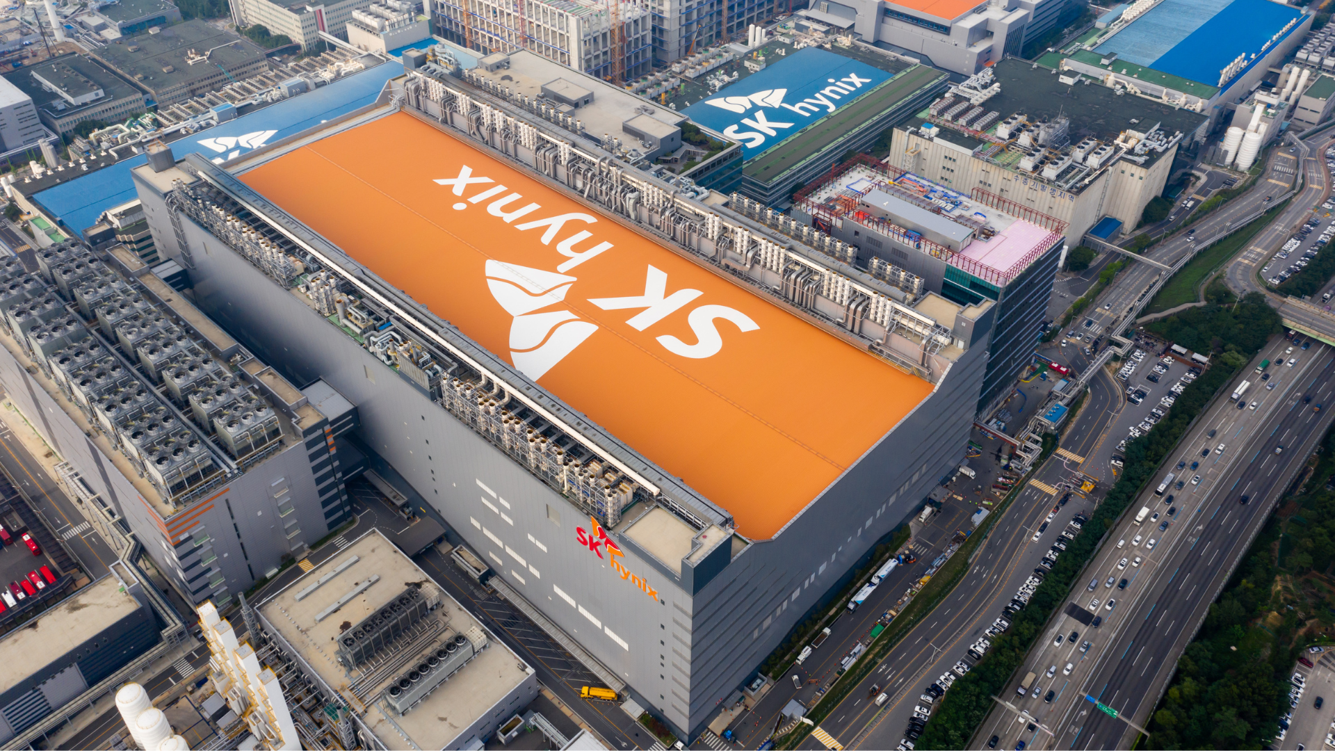
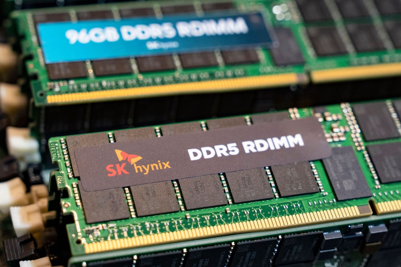
TSMC's water recycling rate reaches 88%, far ahead of Samsung and SK Hynix at roughly 40%.
Samsung shares drop on disappointing earnings; TSMC's pre-earnings pricing move signals shifting semiconductor pricing power.
Samsung Foundry's 2nm-class node built on Gate-All-Around (MBCFET nanosheet) transistors, which Samsung adopted ahead of TSMC at 3nm and now extends to SF2. It improves performance, power, and area over SF3 and adds an Extreme High Density (xHD) library to shrink area further, while staying design-compatible with SF3. SF2 is central to Samsung's bid to close the leading-edge foundry gap with TSMC and win AI and HPC silicon.
Samsung's high-bandwidth memory for AI accelerators, branded Shinebolt. The 12-layer (36GB) stack delivers up to ~1,180 GB/s of bandwidth at 9.2 Gbps per pin. Shinebolt is Samsung's entry in the fierce HBM race against SK Hynix and Micron to supply memory for Nvidia and other AI chips, an area where Samsung has worked to requalify its parts and regain share.
Samsung's next-generation HBM, which entered mass production in early 2026 after qualification sampling to Nvidia. Built on advanced 1c DRAM with a 4nm logic base die, it delivers up to ~2.7x higher throughput and ~40% better power efficiency than HBM3E, with a 2,048-bit interface enabling up to ~3,300 GB/s. Samsung reportedly sold out its entire 2026 HBM4 capacity, underscoring the memory crunch driving the AI buildout.
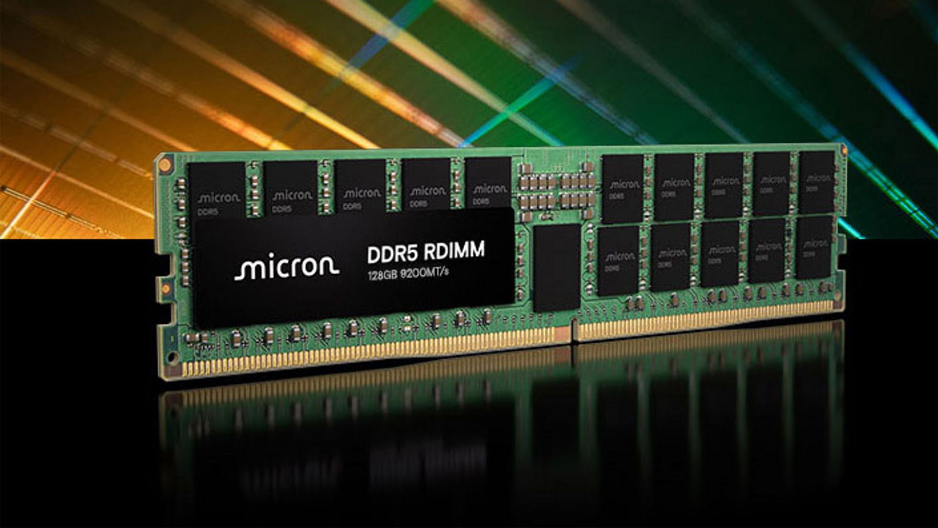
As the world's largest memory maker, Samsung supplies leading-edge DDR5 and LPDDR DRAM on its 1b/1c nodes plus high-layer-count V-NAND flash for SSDs across data-center, mobile, and PC markets. This commodity-and-premium memory franchise, alongside HBM, makes Samsung a primary supplier of the DRAM and storage that AI servers and consumer devices depend on.
152 patents on file, but none with both an extractable figure and an abstract on Google Patents yet.