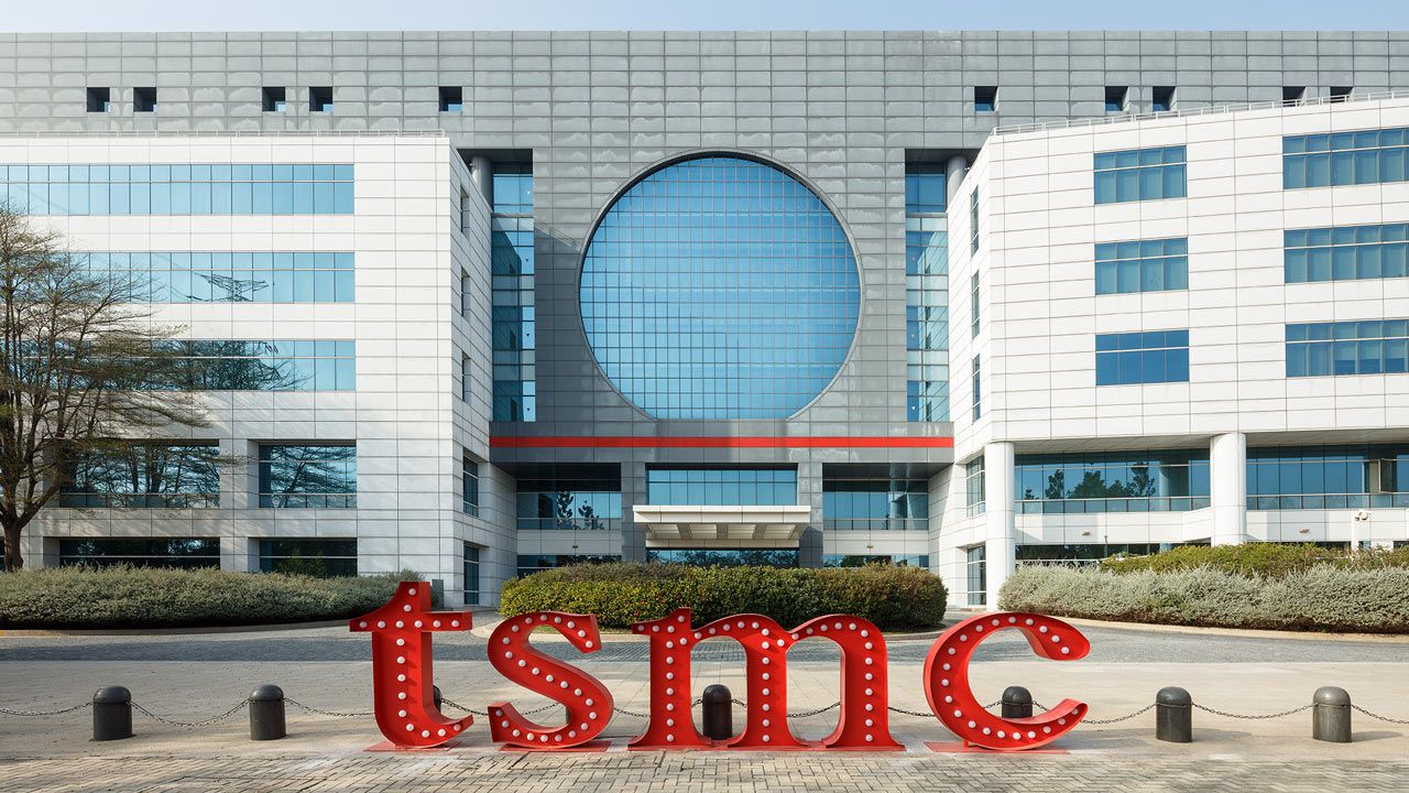
TSMC (TSM) is a publicly traded Foundries company founded in 1987 and based in Hsinchu, Taiwan.
| Date | Stage | Amount | Valuation | Lead investors |
|---|---|---|---|---|
| Oct 8, 1997 | IPO | $595M | — | — |

Taiwan has opened 166 investigations and secured 36 convictions since 2020 for Chinese businesses illegally operating in the island's tech sector via shell companies.

Trump imposes up to 100% tariffs on imported drones and critical components, targeting Chinese-made UAVs and parts.

TSMC's HBM-packaging yield issues open a window for Intel to win foundry customers, analysts say.

IEEE roadmap research finds multi-die assemblies and heterogeneous integration are becoming standard at 2nm and below, driven by AI compute demands outpacing transistor scaling.
TSMC's 2nm-class node and its first to adopt gate-all-around nanosheet transistors, replacing FinFET to deliver higher performance and lower power at the leading edge. N2 entered high-volume manufacturing in late 2025 with good yield, and the N2P/N2U variants extend it with design-technology co-optimization. As the most advanced logic process available to merchant customers, N2 is where the next generation of AI accelerators, CPUs, and flagship mobile SoCs are built.
Chip-on-Wafer-on-Substrate, TSMC's 2.5D advanced-packaging platform that integrates large logic dies with stacks of HBM on a silicon interposer. CoWoS is the indispensable packaging behind virtually every high-end AI accelerator, including Nvidia's GPUs, and its capacity is a primary industry bottleneck. TSMC is scaling to 5.5-reticle interposers today with far larger versions (integrating ~10 compute dies and 20 HBM stacks) on the roadmap.
TSMC's sub-2nm roadmap. A16 pairs nanosheet transistors with Super Power Rail backside power delivery for dense, high-performance HPC designs; A14 introduces a second-generation nanosheet structure targeting another full-node gain (10-15% faster or 25-30% lower power, ~20% denser) with volume production planned for 2028. These nodes extend TSMC's leadership at the physical limits of transistor scaling for future AI and computing silicon.
98 patents on file, but none with both an extractable figure and an abstract on Google Patents yet.